IBM Unveils Nano-Stacking Chips: A Breakthrough for Moore’s Law Extension
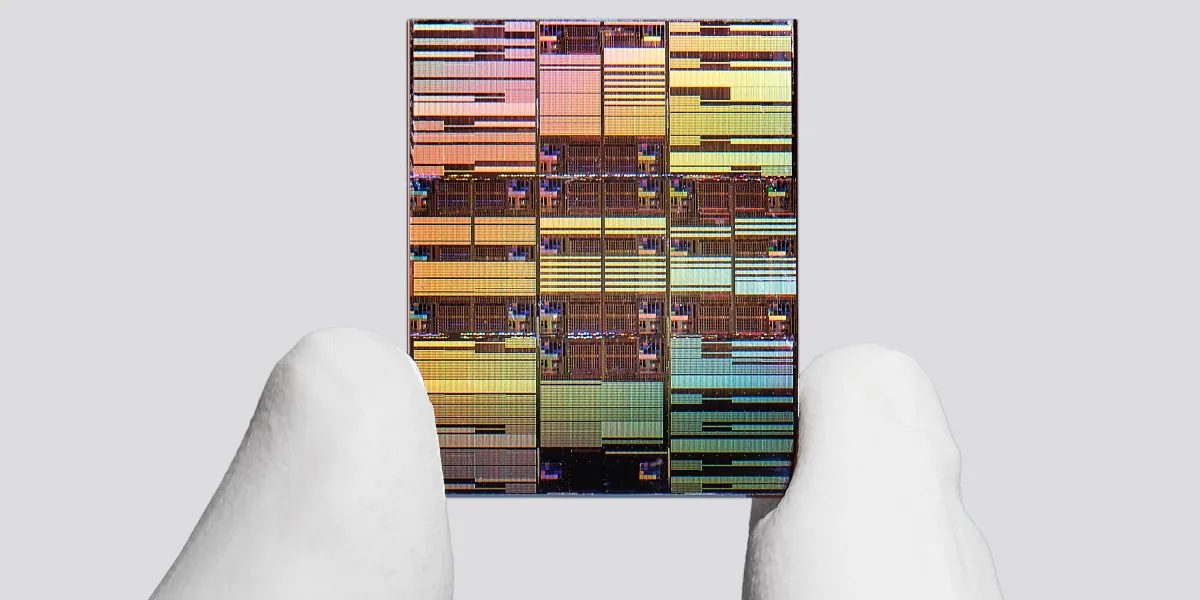
Photo: MIT Technology Review
Quick answer
IBM developed CFET chips with vertically stacked transistors, offering 50% higher performance and up to 70% better energy efficiency than previous solutions.
IBM has unveiled a revolutionary chip architecture based on vertical transistor stacking technology. According to Jay Gambetta, IBM Research Director, this isn’t just an evolutionary improvement but a qualitative leap that could extend Moore’s Law by a decade. The new chips are expected to see widespread use in data centers, where their enhanced energy efficiency will help reduce operational costs.
The new architecture, called CFET (complementary field-effect transistor), involves layer-by-layer transistor fabrication followed by vertical integration. Unlike traditional methods where layers are connected after manufacturing, IBM employs a unique approach with a "checkerboard" arrangement of transistors across layers. This simplifies electrical connections and improves alignment precision, which is critical for modern nanometer-scale technologies.
IBM reports that the new architecture enables chips to perform 50% more operations in the same time while consuming up to 70% less energy. The company plans to collaborate with leading semiconductor manufacturers, including Intel, Samsung, and TSMC, to integrate the technology into mass production. Experts suggest that CFET could become the standard for processors, GPUs, and other microchips used in AI and cloud computing.
Competitors working on similar solutions include AMD with its 3D V-Cache technology and Huawei with the LogicFolding project. However, IBM’s approach stands out due to its higher layer alignment precision, delivering superior performance at smaller transistor sizes. Analysts predict that this new architecture could become a key driver in the development of high-performance computing systems in the coming years.
Common questions
- What is IBM’s nano-stacking technology in chips?
- It’s a method of vertically stacking transistors in multiple layers to increase component density and boost chip performance. IBM uses a unique layer-biasing scheme to simplify electrical connections.
- How will the new chip architecture impact Moore’s Law?
- The technology enables continued transistor miniaturization and increased density, potentially extending Moore’s Law by 10–15 years. This is crucial for AI, cloud computing, and data center advancements.
- What are the key benefits of the new chip architecture?
- Nano-stacking chips deliver up to 50% performance gains and 70% lower power consumption. This is achieved through more efficient transistor placement and optimized electrical connections.
Dzen feed: /feed/dzen.xml · RSS: /feed.xml